|
Overview
Examples
See also:
Custom Backplanes
Standard Backplanes
Boards Design
Schematic Design
Components and Library Management
The way we work with you
Input
Deliverables |
|
Why Active Backplanes?
Although the Active
Backplanes can be considered a subcategory of the Custom defined
Backplanes we consider them a distinct and very well defined
category by itself. This is because, unlike the traditional
backplanes, the active backplanes host active circuitry that
cannot, or it is not desired to, be hosted on the circuit boards
that plug into the backplane. The active circuitry on the backplane
will perform various functions required by the application such
as PCI-to-PCI or PCI-to-PCIExpress bridging, PCIExpress switching,
Ethernet switching, transceivers, magnetics, DC-DC converters
or voltage regulators, I2C and IPMI processors and the examples
can continue.
Traditionally it
was considered that a backplane must be a passive component
of the system in order to yield large MTBF and basically reduced
or no need to repair or replace. Any active component on the
backplane would have only reduced the MTBF. In addition, most
of the backplanes were based on standard bus architectures,
such as VME, VME64x and cPCI, making a backplane usable in various
applications with little or no change at all. Same backplane
in the same system could be used over and over again with new
generations of circuit boards based on a standard bus architecture.
It is also obvious that a backplane can be removed from a system
but only with significant effort and time.
Lately, however, a number of advances in the technologies led to a change in
this philosophy. The MTBF of the active components greatly increased
over the years. The bus architectures, while still in use and
sometimes required as a base physical layer, are increasingly
superseded by newer serial architectures such as VXS, VPX and
PCIExpress that by themselves increase the complexity of the
backplane. The connector's pin and signal density increased
with the speed of the signals. The needs of an application,
given the superior performance and processing power of the new
circuit boards greatly increased and diversified. All these
created the foundation for a new generation of backplanes that
provide additional functionality specific to an application,
working with a specific set of boards and ultimately performing
functions that traditionally belong to the circuit boards.
Such a solution comes in handy when, for example, the processing units that
are required to interface with all the boards in the system
will require a great number of high speed differential signals
that from far exceeds the number of the available pins of the
planned circuit board connector's set. Clearly not all the processing
units can be placed on a single board. Moving the processing
units on the backplane and run all the differential pairs to
the appropriate slots will solve the problem and will increase
the signal integrity by eliminating connector pairs from the
signal's path. Further more, you can put on the backplane your
IP contained in the proprietary circuitry, allowing you to use
off the shelf I/O boards, no longer concerned with how to manage
the signals. You can sell your proprietary backplane and system
to customers for them to use with off the shelf boards.
Although such an
active backplane comes with an increased price tag and a new
thermal approach for the chassis, the benefits will dwarf the
traditional disadvantages.
|
|
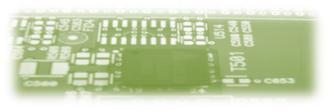
Custom defined active MicroTCA backplane
Description:
DescriptionContent
|
|
|
|
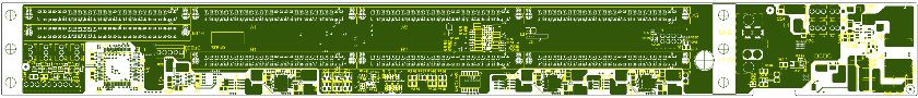
Configurable dual-mode dual cPCI active backplane
Description:
This is a 6U, 7"-wide cPCI based
backplane with two cPCI bus sections of 7 slots working
at 33MHz on 32 bits. The first section is in the P4/P5
zone and the second section in the P1/P2 zone. The requirement
for this specific application was to have the ability
to easily switch between two functional modes.
In the first mode the two cPCI sections
are separate and equipped with own CPU board to control
the cPCI bus. In the second mode the two cPCI
bus sections form a unique bus through a PCI-to-PCI
bridge. This unique cPCI bus is controlled by the CPU
board seated in the first section. The switch between the two modes
should be done when shut down or during a reset, by
a toggle switch on the backplane or an optional switch
mounted on a chassis panel.
We proposed a solution that utilizes
a 32-bit, 33MHz PCI-to-PCI bridge in BGA package and
CMOS Wide Bandwidth Quad 2:1 Muxes in Chip Scale Package
to do the switching of the cPCI signals (see pictures)
. All the circuitry is placed on the backplane utilizing
the available space on the secondary side. The primary
side of the bridge is hard wired to the first bus and
the control signals of the system slot in the first
section.
In the first mode each system slot
controls its own bus section. The bridge is idle, with
output clocks and controlling signals in the secondary
side suspended and the bus lines downstream the bridge
are separated from the second bus by the mux circuits. In the second mode there is only
one CPU equipped in the first system slot, the bridge
is running, the downstream bus lines are connected to
the secondary bus and the clock and control signals
are generated by the bridge for all seven slots of the
second bus. All muxes, bridge reset and clock buffer
are controlled by a single signal generated by the toggle
switch status. LEDs show the mode and verify the actual
mux status. We added latch circuitry triggered
by the Reset signal to secure the toggle switch status
and buffers for the Clock signals.
|
|
|
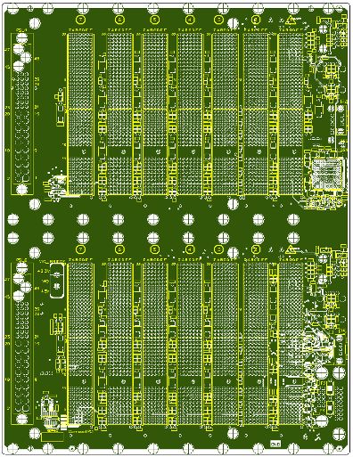
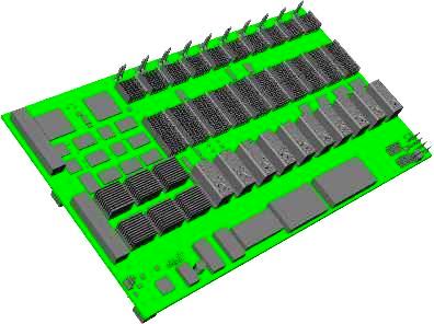
ATCA based PCIExpress switch active backplane
Description:
This is a 10-slot ATCA based backplane.
The application required a processing board equipped
with six PCIe Gen2, 5GT/s 48-lane, 12-port PCIe switches,
two 16-port managed packet processors with the corresponding
transceivers and magnetics, to provide the PCIExpress
links and Gigabit Ethernet base interface to all 10
slots. The challenge came from the fact that such a
board had to provide six X16, one X8 and six X4 PCIExpress
Gen2 links and 20 Gigabit Ethernet links across the
backplane to all 10 boards seated in the ATCA slots.
Given the limited pin's number on a fully populated
ATCA slot such a board could not be built.
Elinktron Technology proposed and
designed a solution that solves both the pin's real
estate issue and the signal integrity issues by placing
all the PCIe and Ethernet circuitry on the backplane.
Thus, all the PCIe links were routed directly from the
switches to the appropriate slots, eliminating a connector's
pair from the signal path. Same for the Gigabit Ethernet
signals. We added to the mix DC-DC converters,
voltage regulators, IPMI control plane to monitor the
local voltages and temperatures all seamlessly integrated
on the backplane. Special attention was given to the
cooling by providing heat sinks where necessary and
providing the 3D models (shown) of the backplane to
the chassis designers for thermal simulations.
|
|
|